SiC基CMOS电路的工艺流程设计与仿真
首发时间:2024-04-22
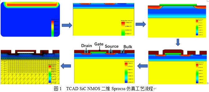
摘要:本文详细介绍了基于SiC CMOS反相器电路的工艺流程设计与仿真过程,阐述了SiC CMOS与传统硅器件在工艺流程上的显著差异。通过使用TCAD软件对NMOS和PMOS进行设计,在TCAD仿真中引入了能带变窄、复合、迁移率和各向异性等物理模型,重点讨论了SiC器件仿真中必须的非完全电离、界面态模型,并详细分析了这些模型对器件及反相器电路仿真结果的影响,为器件的设计与优化提供了更为精确的仿真数据。
For information in English, please click here
Process design and simulation of SiC based CMOS circuits
Abstract:This article provides a detailed description of the process design and simulation process of SiC CMOS inverter circuits, explaining the significant differences in process between SiC CMOS and traditional silicon devices. NMOS and PMOS are designed using TCAD software. Physical models such as band narrowing, recombination, mobility, and anisotropy are introduced in TCAD simulation. It focuses on the necessary physical models for SiC device simulation, including non-complete ionization and interface states. It also analyzes in detail the impact of these models on device and inverter circuit simulation results, providing more accurate simulation data for device design and optimization..
Keywords: IC SiC TCAD model CMOS
论文图表:
引用


No.****
动态公开评议
共计0人参与
勘误表
SiC基CMOS电路的工艺流程设计与仿真
中国科技论文在线 版权所有
网站地图|
在线首页|
在线简介|
服务条款|
联系我们

京公网安备 11040202430024号 京ICP备15006316号-2| 网络出版服务许可证 (总)网出证(京)字第083号 | 文保网安备案号:1101080066


 .txt
.txt .ris
.ris .doc
.doc
评论
全部评论